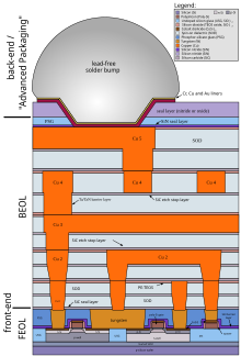

Back end of the line or back end of line (BEOL) is a process in semiconductor device fabrication that consists of depositing metal interconnect layers onto a wafer already patterned with devices. It is the second part of IC fabrication, after front end of line (FEOL). In BEOL, the individual devices (transistors, capacitors, resistors, etc.) are connected to each other according to how the metal wiring is deposited.
Metalization
The individual devices are connected by alternately stacking oxide layers (for insulation purposes) and metal layers (for the interconnect tracks). The vias between layers and the interconnects on the individual layers are thus formed using a structuring process.
Common metals are copper and aluminum. BEOL generally begins when the first layer of metal is deposited on the wafer. BEOL includes contacts, insulating layers (dielectrics), metal levels, and bonding sites for chip-to-package connections. For modern IC processes, more than 10 metal layers can be added in the BEOL.
Before 1998, practically all chips used aluminium for the metal interconnection layers, whereas copper is mostly used nowadays.
Steps
Steps of the BEOL are:
- Silicidation of source and drain regions and the polysilicon region.
- Adding a dielectric (first, lower layer is pre-metal dielectric (PMD) – to isolate metal from silicon and polysilicon), CMP processing it
- Make holes in PMD, make a contacts in them.
- Add metal layer 1
- Add a second dielectric, called the inter-metal dielectric (IMD)
- Make vias through dielectric to connect lower metal with higher metal. Vias filled by Metal CVD process.
- Repeat steps 4–6 to get all metal layers.
- Add final passivation layer to protect the microchip
After BEOL there is a "back-end process" (also called post-fab), which is done not in the cleanroom, often by a different company. It includes wafer test, wafer backgrinding, die separation, die tests, IC packaging and final test.
See also
References
- ^ J. Lienig, J. Scheible (2020). "Chap. 2.9.4: BEOL: Connecting Devices". Fundamentals of Layout Design for Electronic Circuits. Springer. p. 82. doi:10.1007/978-3-030-39284-0. ISBN 978-3-030-39284-0. S2CID 215840278.
- "Copper Interconnect Architecture".
- Karen A. Reinhardt and Werner Kern (2008). Handbook of Silicon Wafer Cleaning Technology (2nd ed.). William Andrew. p. 202. ISBN 978-0-8155-1554-8.
Further reading
- "Chapter 11: Back End Technology". Silicon VLSI Technology: Fundamentals, Practice, and Modeling. Prentice Hall. 2000. pp. 681–786. ISBN 0-13-085037-3.
- "Chapter 7.2.2: CMOS Process Integration: Backend-of-the-line Integration". CMOS: Circuit Design, Layout, and Simulation. Wiley-IEEE. 2010. pp. 199–208 . ISBN 978-0-470-88132-3.
- "Chapter 2: Technology Know-How: From Silicon to Devices". Fundamentals of Layout Design for Electronic Circuits, by Lienig, Scheible, Springer, doi:10.1007/978-3-030-39284-0ISBN 978-3-030-39284-0, 2020. p. 82 (2.9.4 BEOL: Connecting Devices)