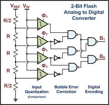
A flash ADC (also known as a direct-conversion ADC) is a type of analog-to-digital converter that uses a linear voltage ladder with a comparator at each "rung" of the ladder to compare the input voltage to successive reference voltages. Often these reference ladders are constructed of many resistors; however, modern implementations show that capacitive voltage division is also possible. The output of these comparators is generally fed into a digital encoder, which converts the inputs into a binary value (the collected outputs from the comparators can be thought of as a unary value).
Benefits and drawbacks
Flash converters are high-speed compared to many other ADCs, which usually narrow in on the correct answer over a series of stages. Compared to these, a flash converter is also quite simple and, apart from the analog comparators, only requires logic for the final conversion to binary.
For best accuracy, a track-and-hold circuit is often inserted in front of an ADC input. This is needed for many ADC types (like successive approximation ADC), but for flash ADCs, there is no real need for this because the comparators are the sampling devices.
A flash converter requires many comparators compared to other ADCs, especially as the precision increases. For example, a flash converter requires comparators for an n-bit conversion. The size, power consumption, and cost of all those comparators make flash converters generally impractical for precisions much greater than 8 bits (255 comparators). In place of these comparators, most other ADCs substitute more complex logic and/or analog circuitry that can be scaled more easily for increased precision.
Implementation

Flash ADCs have been implemented in many technologies, varying from silicon-based bipolar (BJT) and complementary metal–oxide FETs (CMOS) technologies to rarely used III-V technologies. This type of ADC is often used as a first medium-sized analog circuit verification.
The earliest implementations consisted of a reference ladder of well-matched resistors connected to a reference voltage. Each tap at the resistor ladder is used for one comparator, possibly preceded by an amplification stage, and thus generates a logical 0 or 1 depending on whether the measured voltage is above or below the reference voltage of the voltage divider. The reason to add an amplifier is twofold: it amplifies the voltage difference. It, therefore, suppresses the comparator offset and the kick-back noise of the comparator towards the reference ladder is also strongly suppressed. Typically designs from 4-bit up to 6-bit and sometimes 7-bit are produced.
Designs with power-saving capacitive reference ladders have been demonstrated. In addition to clocking the comparator(s), these systems also sample the reference value on the input stage. As the sampling is done at a very high rate, the leakage of the capacitors is negligible.
Recently, offset calibration has been introduced into flash ADC designs. Instead of high-precision analog circuits (which increase the component size to suppress variation), comparators with relatively large offset errors are measured and adjusted. Then, a test signal is applied, and the offset of each comparator is calibrated to below the LSB value of the ADC.
Another improvement to many flash ADCs is the inclusion of digital error correction. When the ADC is used in harsh environments or constructed from very small integrated circuit processes, there is a heightened risk that a single comparator will randomly change state resulting in a wrong code. Bubble error correction is a digital correction mechanism that prevents a comparator that has, for example, tripped high from reporting logic high if it is surrounded by comparators that are reporting logic low.
Folding ADC
The number of comparators can be reduced somewhat by adding a folding circuit in front, making a so-called folding ADC. Instead of using the comparators in a flash ADC only once, the folding ADC re-uses the comparators multiple times during a ramp input signal. If a m-times folding circuit is used in an n-bit ADC, the actual number of comparator can be reduced from to (there is always one needed to detect the range crossover). Typical folding circuits are the Gilbert multiplier and analog wired-OR circuits.
Application
The very high sample rate of this type of ADC enables high-frequency applications (typically in a few GHz range) like radar detection, wideband radio receivers, electronic test equipment, and optical communication links. Moreover, the flash ADC is often embedded in a large IC containing many digital decoding functions.
Also, a small flash ADC circuit may be present inside a delta-sigma modulation loop.
Flash ADCs are also used in NAND flash memory, where up to 3 bits are stored per cell as 8 voltages level on floating gates.
References
- Analog-to-Digital Conversion
- Understanding Flash ADCs
- "Integrated Analog-to-Digital and Digital-to-Analog Converters", R. van de Plassche, ADCs, Kluwer Academic Publishers, 1994.
- "A Precise Four-Quadrant Multiplier with Subnanosecond Response", Barrie Gilbert, IEEE Journal of Solid-State Circuits, Vol. 3, No. 4 (1968), pp. 365–373
 comparators for an n-bit conversion. The size, power consumption, and cost of all those comparators make flash converters generally impractical for precisions much greater than 8 bits (255 comparators). In place of these comparators, most other ADCs substitute more complex
  (there is always one needed to detect the range crossover). Typical folding circuits are the