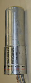
A semiconductor detector in ionizing radiation detection physics is a device that uses a semiconductor (usually silicon or germanium) to measure the effect of incident charged particles or photons.
Semiconductor detectors find broad application for radiation protection, gamma and X-ray spectrometry, and as particle detectors.
Detection mechanism
In semiconductor detectors, ionizing radiation is measured by the number of charge carriers set free in the detector material which is arranged between two electrodes, by the radiation. Ionizing radiation produces free electrons and electron holes. The number of electron-hole pairs is proportional to the energy of the radiation to the semiconductor. As a result, a number of electrons are transferred from the valence band to the conduction band, and an equal number of holes are created in the valence band. Under the influence of an electric field, electrons and holes travel to the electrodes, where they result in a pulse that can be measured in an outer circuit, as described by the Shockley-Ramo theorem. The holes travel in the opposite direction and can also be measured. As the amount of energy required to create an electron-hole pair is known, and is independent of the energy of the incident radiation, measuring the number of electron-hole pairs allows the energy of the incident radiation to be determined.
The energy required to produce electron-hole-pairs is very low compared to the energy required to produce paired ions in a gas detector. Consequently, in semiconductor detectors the statistical variation of the pulse height is smaller and the energy resolution is higher. As the electrons travel fast, the time resolution is also very good, and is dependent upon rise time. Compared with gaseous ionization detectors, the density of a semiconductor detector is very high, and charged particles of high energy can give off their energy in a semiconductor of relatively small dimensions.
Detector types
| This section does not cite any sources. Please help improve this section by adding citations to reliable sources. Unsourced material may be challenged and removed. (November 2020) (Learn how and when to remove this message) |
Silicon detectors

Most silicon particle detectors work, in principle, by doping narrow (usually around 100 micrometers wide) silicon strips to turn them into diodes, which are then reverse biased. As charged particles pass through these strips, they cause small ionization currents that can be detected and measured. Arranging thousands of these detectors around a collision point in a particle accelerator can yield an accurate picture of what paths particles take. Silicon detectors have a much higher resolution in tracking charged particles than older technologies such as cloud chambers or wire chambers. The drawback is that silicon detectors are much more expensive than these older technologies and require sophisticated cooling to reduce leakage currents (noise source). They also suffer degradation over time from radiation, however, this can be greatly reduced thanks to the Lazarus effect.
Diamond detectors
Diamond detectors have many similarities with silicon detectors but are expected to offer significant advantages – in particular a high radiation hardness and very low drift currents. They are also suited to neutron detection. At present, however, they are much more expensive and more difficult to manufacture.
Germanium detectors

Germanium detectors are mostly used for gamma spectroscopy in nuclear physics, as well as x-ray spectroscopy. While silicon detectors cannot be thicker than a few millimeters, germanium can have a sensitive layer (depletion region) thickness of centimeters, and therefore can be used as a total absorption detector for gamma rays up to a few MeV. These detectors are also called high-purity germanium detectors (HPGe) or hyperpure germanium detectors. Before current purification techniques were refined, germanium crystals could not be produced with purity sufficient to enable their use as spectroscopy detectors. Impurities in the crystals trap electrons and holes, ruining the performance of the detectors. Consequently, germanium crystals were doped with lithium ions (Ge(Li)), in order to produce an intrinsic region in which the electrons and holes would be able to reach the contacts and produce a signal.
When germanium detectors were first developed, only very small crystals were available. Low efficiency was the result, and germanium detector efficiency is still often quoted in relative terms to a "standard" 3″ x 3″ NaI(Tl) scintillation detector. Crystal growth techniques have since improved, allowing detectors to be manufactured that are as large as or larger than commonly available NaI crystals, although such detectors cost more than €100,000 (US$113,000).
As of 2012, HPGe detectors commonly use lithium diffusion to make an n ohmic contact, and boron implantation to make a p contact. Coaxial detectors with a central n contact are referred to as n-type detectors, while p-type detectors have a p central contact. The thickness of these contacts represents a dead layer around the surface of the crystal within which energy depositions do not result in detector signals. The central contact in these detectors is opposite to the surface contact, making the dead layer in n-type detectors smaller than the dead layer in p-type detectors. Typical dead layer thicknesses are several hundred micrometers for a Li diffusion layer and a few tenths of a micrometer for a B implantation layer.
The major drawback of germanium detectors is that they must be cooled to liquid nitrogen temperatures to produce spectroscopic data. At higher temperatures, the electrons can easily cross the band gap in the crystal and reach the conduction band, where they are free to respond to the electric field, producing too much electrical noise to be useful as a spectrometer. Cooling to liquid nitrogen temperature (77K) reduces thermal excitations of valence electrons so that only a gamma ray interaction can give an electron the energy necessary to cross the band gap and reach the conduction band. Cooling with liquid nitrogen is inconvenient, as the detector requires hours to cool down to operating temperature before it can be used, and cannot be allowed to warm up during use. Ge(Li) crystals could never be allowed to warm up, as the lithium would drift out of the crystal, ruining the detector. HPGe detectors can be allowed to warm up to room temperature when not in use.
Commercial systems became available that use advanced refrigeration techniques (for example pulse tube refrigerator) to eliminate the need for liquid nitrogen cooling.
Germanium detectors with multi-strip electrodes, orthogonal on opposing faces, can indicate the 2-D location of the ionization trail within a large single crystal of Ge. Detectors like this have been used in COSI balloon-born astronomy missions (NASA, 2016) and will be used in an orbital observatory (NASA, 2025) Compton Spectrometer and Imager (COSI).
Because germanium detectors are highly efficient in photon detection, they can be used for a variety of additional applications. High-purity germanium detectors are used by Homeland Security to differentiate between naturally occurring radioactive material (NORM) and weaponized or otherwise harmful radioactive material. They are also used in monitering the environment due to the concern of the use of nuclear power. Finally, high-purity germanium detectors are used for medical imaging and nuclear physics research, making them a rather diverse detector as far as applications go.
Cadmium telluride and cadmium zinc telluride detectors
Cadmium telluride (CdTe) and cadmium zinc telluride (CZT) detectors have been developed for use in X-ray spectroscopy and gamma spectroscopy. The high density of these materials means they can effectively attenuate X-rays and gamma-rays with energies of greater than 20 keV that traditional silicon-based sensors are unable to detect. The wide band gap of these materials also means they have high resistivity and are able to operate at, or close to, room temperature (~295K) unlike germanium-based sensors. These detector materials can be used to produce sensors with different electrode structures for imaging and high-resolution spectroscopy. However, CZT detectors are generally unable to match the resolution of germanium detectors, with some of this difference being attributable to poor positive charge-carrier transport to the electrode. Efforts to mitigate this effect have included the development of novel electrodes to negate the need for both polarities of carriers to be collected.
Integrated Systems
Semiconductor detectors are often commercially integrated into larger systems for various radiation measurement applications.
Automated Sample Changing for Germanium Detectors

Gamma spectrometers using HPGe detectors are often used for measurement of low levels of gamma-emitting radionuclides in environmental samples, which requires a low background environment, usually achieved by enclosing the sample and detector in a lead shield known as a 'lead castle'. Automated systems have been developed to sequentially move a number of samples into and out of the lead castle for measurement. Due to the complexities of opening the shield and moving the samples, this automation has traditionally been expensive, but lower-cost autosamplers have recently been introduced.
Radioactive Waste Assay Machines
Semiconductor detectors especially HPGe are often integrated into devices for characterising packaged radioactive waste. This can be as simple as detectors being mounted on a moveable platform to be brought to an area for in-situ measurements and paired with shielding to restrict the field-of-view of the detector to the area of interest for one-shot "open detector geometry" measurements, or for waste in drums, systems such as the Segmented Gamma Scanner (SGS) combine a semiconductor detector with integrated mechatronics to rotate the item and scan the detector across different sections. If the detector field of view is scanned across small areas of the item in multiple axes as is done with a Tomographic Gamma Scanner (TGS), Tomography can be used to extract 3D information about the density and gamma emissions of the item.
Gamma Cameras
Semiconductor detectors are used in some Gamma Cameras and Gamma imaging systems
See also
- Lazarus effect
- Pandemonium effect
- Synthetic diamonds
- Total absorption spectroscopy
- X-ray spectroscopy
- Microstrip detector
- Hybrid pixel detector
- Liulin type instruments
References
- Knoll, G.F. (1999). Radiation Detection and Measurement (3rd ed.). Wiley. p. 365. ISBN 978-0-471-07338-3.
- Knoll, p119
- Kapustinsky, Jon S. (17 November 2010). "Sensors/FPHX Readout Chip WBS 1.4.1/1.4.2" (PDF). Retrieved 7 August 2017.
{{cite journal}}: Cite journal requires|journal=(help) - Sangsingkeow, Pat; Berry, Kevin D; Dumas, Edward J; Raudorf, Thomas W; Underwood, Teresa A (June 2003). "Advances in germanium detector technology". Nuclear Instruments and Methods in Physics Research Section A: Accelerators, Spectrometers, Detectors and Associated Equipment. 505 (1–2): 183–186. Bibcode:2003NIMPA.505..183S. doi:10.1016/s0168-9002(03)01047-7. ISSN 0168-9002.
- "Deciphering Radiation Alarms: Using High Purity Germanium Detectors for Nuclear Security". www.iaea.org. 18 December 2020. Retrieved 6 May 2024.
- "High-Sensitivity Detectors | Homeland Security". www.dhs.gov. Retrieved 6 May 2024.
- "Document Display | NEPIS | US EPA". nepis.epa.gov. Retrieved 6 May 2024.
- Cooper, R.J.; Amman, M.; Luke, P.N.; Vetter, K. (September 2015). "A prototype High Purity Germanium detector for high resolution gamma-ray spectroscopy at high count rates". Nuclear Instruments and Methods in Physics Research Section A: Accelerators, Spectrometers, Detectors and Associated Equipment. 795: 167–173. Bibcode:2015NIMPA.795..167C. doi:10.1016/j.nima.2015.05.053. ISSN 0168-9002.
- Luke, P. N. (1 November 1994). "Unipolar charge sensing with coplanar electrodes -- Application to semiconductor detectors". doi:10.2172/34411. OSTI 34411.
{{cite journal}}: Cite journal requires|journal=(help) - J. S. Kapustinsky, Nucl. Instrum. Methods A 617 (2010) 546 – 548.
- "Robotic Gamma Spectrometer with sample changer – Nuclear System".
- Carvalho, Matheus (2018). "Auto-HPGe, an autosampler for gamma-ray spectroscopy using high-purity germanium (HPGe) detectors and heavy shields". HardwareX. 4: e00040. doi:10.1016/j.ohx.2018.e00040.
- ISO 19017:2015
- LALP-91-011, Application Note, Segmented Gamma-Ray Scanner
- LA-UR-93-1637, Tomographic gamma scanning (TGS) to measure inhomogeneous nuclear material matrices from future fuel cycles, LANL, 1993
- "H100 - H3D, Inc".
External links
- Silicon Detector powerpoint delivered for EDIT (Excellence in Detectors and Instrumentation Technologies) 2011 at CERN, M. Krammer, F. Hartmann.
| Radiation protection | |
|---|---|
| Main articles | |
| Measurement quantities and units | |
| Instruments and measurement techniques | |
| Protection techniques | |
| Organisations | |
| Regulation | |
| Radiation effects | |
| See also the categories Medical physics, Radiation effects, Radioactivity, Radiobiology, and Radiation protection | |